Highlights
Susi, T., Identifying and manipulating single atoms with scanning transmission electron microscopy, Chemical Communications 58, 12274-12285 (2022). doi:10.1039/D2CC04807H
Susi, T., Meyer, J.C., Kotakoski, J., Reshaping low-dimensional materials down to the atomic level with electron irradiation, Ultramicroscopy 180, 163-172 (2017). doi:10.1016/ j.ultramic.2017.03.005
Susi, T., et al., Silicon–Carbon Bond Inversions Driven by 60-keV Electrons in Graphene, Phys. Rev. Lett. 113, 115501 (2014). doi: 10.1103/
PhysRevLett.113.115501
Manipulating individual atoms
Electrons are fundamentally different to light as a microscopy probe since they carry significant momentum and thus can case changes in the atomic structure. This can be used to manipulate materials on the atomic scale using the Ångström-sized electron probe of a scanning transmission electron microscope (STEM).
Great progress has been made in several materials including graphene, carbon nanotubes, and crystalline silicon in the eight years since the discovery of electron-beam manipulation, but the important challenges that remain will determine how far we can expect to progress in the near future.
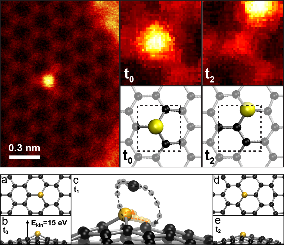
A silicon atom embedded in the graphene lattice shows bright in the STEM MAADF scattering contrast. While imaging the area, the silicon atom "jumps" to the next lattice site, with no atoms lost from the structure. The mechanism is explained by atomistic simulations which reveal the complex out-of-plane dynamics responsible for the Si-C bond inversion.


